Modern-day information and communication technologies (ICT) are well known for producing large amounts of heat, which is undesirable for both energy efficiency and environmental sustainability.
Research has shown that a significant portion of the energy utilized by computer processors isn’t spent on performing calculations but rather on transferring bytes between memory and the processor. This energy consumption contributes to the high CO2 footprint of the global ICT ecosystem. In fact, the CO2 footprint of the ICT sector is comparable to that of the aviation industry.
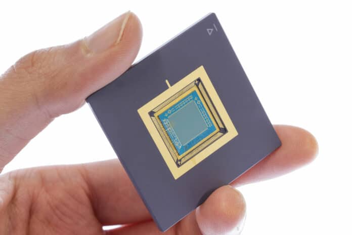
Recently, researchers from EPFL’s School of Engineering in the Laboratory of Nanoscale Electronics and Structures (LANES) have developed a new processor that addresses this inefficiency by integrating data processing and storage onto a single device, a so-called in-memory processor.
The team made a breakthrough by creating the first large-scale in-memory processor based on a two-dimensional semiconductor material to comprise more than 1000 transistors, a significant achievement for industrial production.
Developed roughly 80 years ago, the von Neumann architecture is the basis of almost all computing done today.
However, according to Andras Kis, who led the study, the main reason for today’s CPUs’ low efficiency is this von Neumann architecture in which the components used to perform calculations and to store data are physically separated. This means processors need to retrieve data from the memory to perform calculations, which involves moving electrical charges, charging and discharging capacitors, and transmitting currents along lines – all of which dissipate energy.
This architecture was reasonable until about 20 years ago because different types of devices were required for data storage and processing. But the von Neumann architecture is increasingly being challenged by more efficient alternatives that merge storage and processing into more universal in-memory processors.
Instead of silicon, the most widely used semiconductor in today’s computer processors, EPFL researchers have used molybdenum disulfide (MoS2), a semiconductor material. MoS2 forms a stable monolayer, just three atoms thick that only interacts weakly with its surroundings. Its thinness offers the potential to produce extremely compact devices in 2D.
The MoS2-based in-memory processor combines 1024 elements onto a one-by-one-centimeter chip. Each element comprises a 2D MoS2 transistor and a floating gate that stores a charge to control the conductivity of each transistor. By setting the conductivity of each transistor, researchers can perform analog vector-matrix multiplication in a single step by applying voltages to their processors and measuring the output.
“The key advance in going from a single transistor to over 1000 was the quality of the material that we can deposit. After a lot of process optimization, we can now produce entire wafers covered with a homogenous layer of uniform MoS2. This lets us adopt industry standard tools to design integrated circuits on a computer and translate these designs into physical circuits, opening the door to mass production,” says Andras Kis in the press release.
According to researchers, this new architecture could help revive electronics fabrication in Europe. Instead of competing in silicon wafer fabrication, they believe that their research opens up new possibilities for non-von Neumann processing architecture for AI accelerators and other emerging applications.
