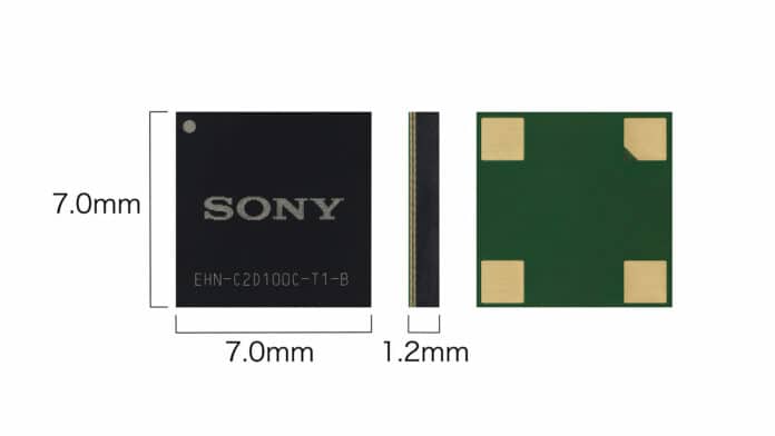
As the number of small Internet of Things (IoT) devices continues to increase, energy harvesting is gaining more attention as a potential solution to address the power consumption challenge. Many IoT nodes consume only milliwatts or microwatts individually but add up in volume to a major power draw.
To combat this issue, various energy harvesting systems are being developed to harness alternative sources of energy, ranging from solar energy, light, and heat to vibration. Instead, Sony’s new creation opts for electromagnetic noise that all electrical equipment generates.
In a groundbreaking development, Sony Semiconductor Solutions (SSS) has announced a new energy-harvesting module that efficiently generates power from electromagnetic wave noise for IoT devices.
The new module is designed to generate high-efficiency power from electromagnetic wave noise, using technology developed by SSS during the tuner development process. This innovative technology can utilize constant electromagnetic wave noise generated by various electronic devices, such as robots in factories, monitors and lighting in offices, and monitors and TVs in stores and homes, to provide a stable power supply for low-power consumption IoT sensors and communication equipment.
The new energy-harvesting module boasts a unique architecture integrating an antenna and a high-efficiency rectifier circuit. The antenna captures electromagnetic wave noise from the metallic parts of electronic devices, which is then converted into a direct current with notably improved efficiency by the rectifier circuit.
While the exact efficiency data of the module is not yet available, it is notable that the technology can convert electromagnetic wave noise in a range of several Hz to 100 MHz into electrical energy and supply power to low-power consumption IoT sensors and communications equipment or to charge batteries.
“This is the industry’s first energy harvesting technology based on this method that achieves highly efficient power generation. By efficiently utilizing previously ignored electromagnetic wave noise as a new power source, it enables a stable power supply for equipment,” the company claims.
Sony’s innovation stands out for its compact footprint, measuring at just 7 mm x 7 mm x 1.2 mm. The compact design allows for greater freedom of installation. Also, as long as electronic devices are powered, energy can be harvested even while they are not in active use, making this technology promising in a wide variety of usage situations such as factories, offices, stores, and homes, both indoors and outdoors.
Sony Semiconductor Solutions has not yet released full specifications for the module, but it claims that the module can harvest from several dozen μW to several dozen mW of power from a range of common devices, including household appliances, computers, lighting equipment, vending machines, elevators, automobiles, and industrial equipment. The company also claims that the module can act as a remote sensor for predictive maintenance, monitoring changes in the harvested energy levels to infer the status of the noise-generating devices.
Sony looks forward to working with partners from various industries to develop products based on this technology, which shows promise across a wide variety of applications.
