
Samsung announced that it has started initial production of its 3-nanometer (nm) process node applying Gate-All-Around (GAA) transistor architecture, beating rival TSMC, which expects to begin making chips with its N3 node generation later this year.
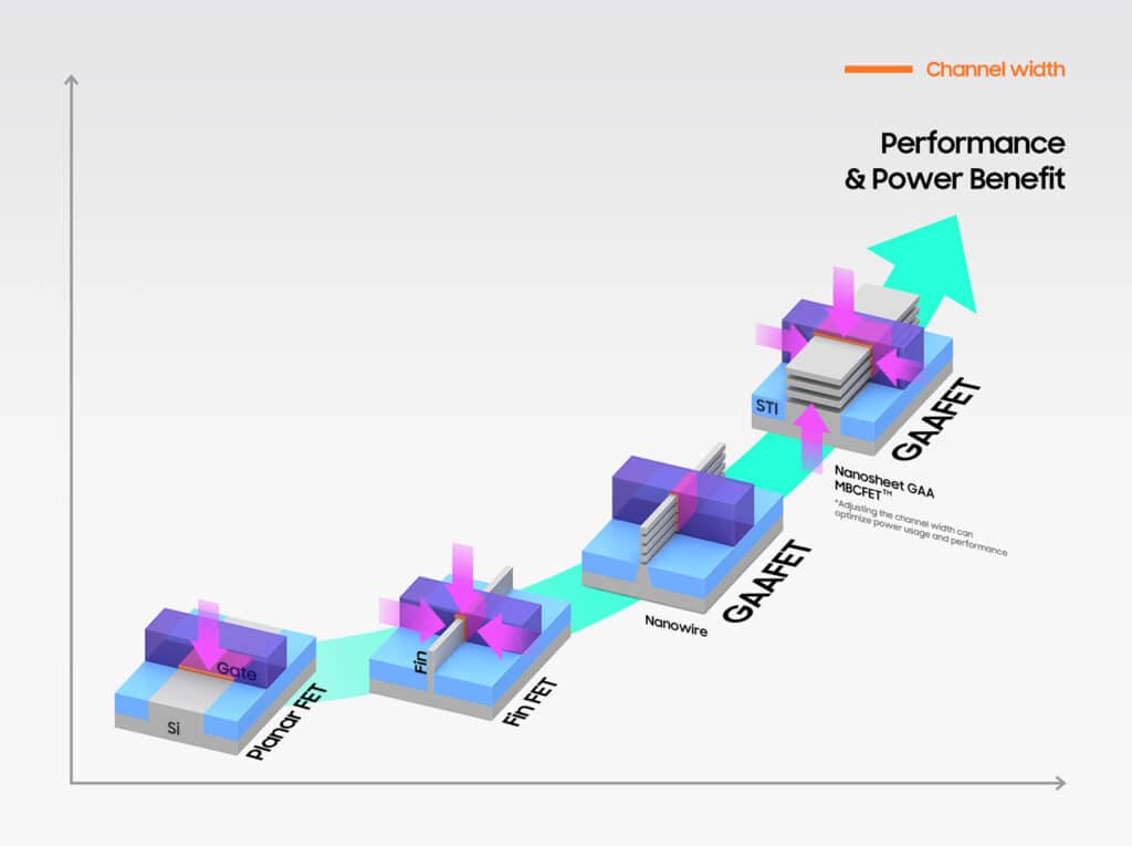
Samsung’s 3nm process node introduces what the firm calls Multi-Bridge-Channel FET (MBCFET) technology for the first time ever. This is Samsung’s version of the GAA transistor architecture, where the gate material wraps around the conducting channel. The technology defies the performance limitations of FinFET, improving power efficiency by reducing the supply voltage level while also enhancing performance by increasing drive current capability.
The company’s proprietary technology utilizes nanosheets with wider channels, which allow higher performance and greater energy efficiency compared to GAA technologies using nanowires with narrower channels. Utilizing the 3nm GAA technology, Samsung will be able to adjust the channel width of the nanosheet in order to optimize power usage and performance to meet various customer needs.
Compared to the 5nm process, the chip manufactured using the first-generation 3nm process can reduce power consumption by up to 45%, improve performance by 23% and reduce the area by 16% compared to 5nm. The second-generation 3nm process is to reduce power consumption by up to 50%, improve performance by 30% and reduce the area by 35%, according to the company.
Samsung is starting the first application of the nanosheet transistor with semiconductor chips for high-performance, low-power computing applications and plans to expand to mobile processors.
The announcement of the start of production confirms Samsung’s technological advantage over rival TSMC, which still uses 3-nanometer FinFET transistors.
“Samsung has grown rapidly as we continue to demonstrate leadership in applying next-generation technologies to manufacturing, such as the foundry industry’s first High-K Metal Gate, FinFET, as well as EUV. We seek to continue this leadership with the world’s first 3nm process with the MBCFET,” said Dr. Siyoung Choi, President and Head of Foundry Business at Samsung Electronics. “We will continue active innovation in competitive technology development and build processes that help expedite achieving maturity of the technology.”