
Solar panels rely on semiconductor devices, or solar cells, to convert energy from the sun into electricity. To generate electricity, solar cells need an electric field to separate positive charges from negative charges.
To create this field, manufacturers typically dope the solar cell with chemicals so that one layer of the device bears a positive charge and another layer has a negative charge. This multi-layered design ensures that electrons flow from the negative side of a device to the positive side – a key factor in device stability and performance. This adds extra cost to cell manufacturing.
Now, a team of researchers at DOE’s Lawrence Berkeley National Laboratory (Berkeley Lab), in collaboration with UC Berkeley, has demonstrated a unique material that can be used as a simpler approach to solar cell manufacturing. The crystalline solar material with a built-in electric field – a property enabled by what scientists call “ferroelectricity.” The breakthrough could make solar cell devices less expensive, easier, and more efficient.
Grown in the lab from cesium germanium tribromide (CsGeBr3 or CGB), the new ferroelectric material opens the door to an easier approach to making solar cell devices. CGB crystals are inherently polarized, where one side of the crystal builds up positive charges and the other side builds up negative charges, with no doping required.
CGB is also a lead-free “halide perovskite,” an emerging class of affordable and easy-to-make solar materials. Typically, the best-performing halide perovskites naturally contain the element lead. The lead remnants from perovskite solar material production and disposal could contaminate the environment and present public health concerns. Researchers discovered the new material eschews lead without compromising performance.
They say CGB could also advance a new generation of switching devices, sensors, and super-stable memory devices that respond to light. They also theorized that the asymmetric placement of germanium in the center of the crystal would create a potential that separates positive electrons from negative electrons to produce electricity.
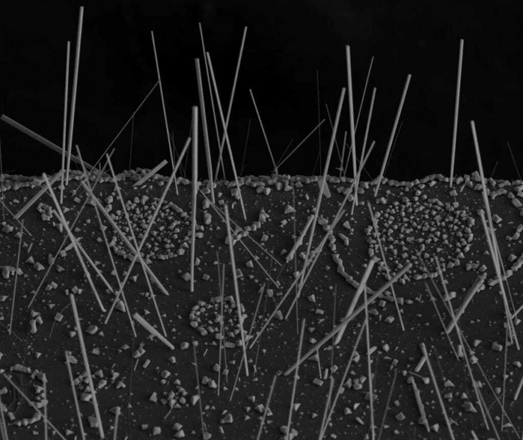
To find out, the team grew tiny nanowires (100 to 1,000 nanometers in diameter) and nanoplates (around 200 to 600 nanometers thick and 10 microns wide) of single-crystalline CGB with exceptional control and precision.
X-ray and electron microscopy experiments revealed CGB’s asymmetrical crystalline structure, a signal of ferroelectricity. Meanwhile, electrical measurement experiments revealed a switchable polarity in CGB, satisfying yet another requirement for ferroelectricity.
But in the final test, the researchers found that CGB’s light absorption is tunable – spanning the spectrum of visible to ultraviolet light (1.6 to 3 electron volts), an ideal range for coaxing high energy conversion efficiencies in a solar cell, said co-senior author Peidong Yang. Yang further says there is still more work to be done before the CGB material can make its debut in a commercial solar device.